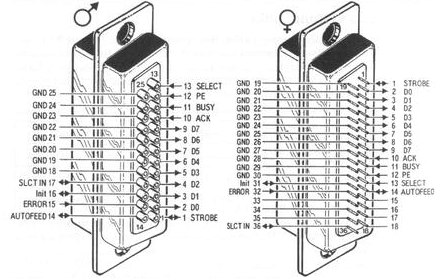
Parallel port usually uses two types of connectors:
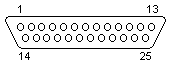
- 25 pin D-sub female conector (figure 1), which is usually
part of a PC motherboard.
- 36 pin Centronics female conector, which is usually used
in printers and others peripheral devices.
In figure 1., there is description of each pin and signal, which
represents them. There is pertinence each pin to PC register (Data,Status,
Control) for both connectors. Standard IEEE1284 defines also 36-pin
connector similar with Centronics, but smaller.
Fig. 1. LPT signals assigment to 25-pin D-SUB connector
|
Pin No (D-Type 25) |
Pin No (Centronics) |
SPP Signal |
Direction In/out |
Register |
Hardware Inverted |
| 1 |
1 |
nStrobe |
In/Out |
Control |
Yes |
| 2 |
2 |
Data 0 |
Out |
Data |
|
| 3 |
3 |
Data 1 |
Out |
Data |
|
| 4 |
4 |
Data 2 |
Out |
Data |
|
| 5 |
5 |
Data 3 |
Out |
Data |
|
| 6 |
6 |
Data 4 |
Out |
Data |
|
| 7 |
7 |
Data 5 |
Out |
Data |
|
| 8 |
8 |
Data 6 |
Out |
Data |
|
| 9 |
9 |
Data 7 |
Out |
Data |
|
| 10 |
10 |
nAck |
In |
Status |
|
| 11 |
11 |
Busy |
In |
Status |
Yes |
| 12 |
12 |
Paper-Out / Paper-End |
In |
Status |
|
| 13 |
13 |
Select |
In |
Status |
|
| 14 |
14 |
nAuto-Linefeed |
In/Out |
Control |
Yes |
| 15 |
32 |
nError / nFault |
In |
Status |
|
| 16 |
31 |
nInitialize |
In/Out |
Control |
|
| 17 |
36 |
nSelect-Printer / nSelect-In |
In/Out |
Control |
Yes |
| 18 - 25 |
19-30 |
Ground |
Gnd |
|
|
Tab 1. Pin Assignments of the D-Type 25 pin Parallel Port Connector
Note: Pins table for LPT with their
names is possible to download in Documents section or with figures of Centronics port pins resolution in LPT port pins resolution
for IEEE 1284 standard.
Signals definition
Output signals
of the parallel port are defined as typical TTL logical level
signals. High level is defined by voltage from 3.5V to 5.5V
and low level from 0V to 0.4V (figure 2.).
Diferent values of maximal load currents of the parallel port
are done by physical realization of the port. Maximal current
takes from pins should be from range 4mA and 20mA. Therefore
it's better use a buffer between PC and peripheral device. |
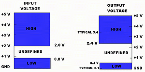
Fig. 2. TTL voltage level definition (input
voltage, output voltage) |
| Rules for safe work against
port destruction |
PC port addresses |
In comparison with serial
port the parallel port can be destroyed very easily, because
outputs aren't usually protected against overload and overcharge.
Therefore it's better to keep following precautions:
-
Devices should be connected only to switch off
power supplies of computers.
-
At inputs there should be brought only voltage
betwen 0 and 5V.
-
Outputs should make short circuit or should be
connected to others outputs.
-
Outputs should be contacted with strange voltage.
-
In work with parallel port should be kept all
outlines for minimalization of static electricity.
|
For PC parallel ports it's
defined and used 3 basic addresses which show table 2.
|
Address |
Notes: |
|
3BCh - 3BFh |
Used for Parallel Ports which were incorporated on to Video
Cards - Doesn't support ECP addresses |
| 378h - 37Fh |
Usual Address For LPT 1 |
| 278h - 27Fh |
Usual Address For LPT 2 |
Tab 2. Table 2 Port Addresses
Address 3BCh was originally used for old Video cards and nowadays
it isn't used. In BIOS there can be found port addresses in
memory accirding to table 3.
|
Start Address
|
Function
|
| 0000:0408 |
LPT1's Base Address |
| 0000:040A |
LPT2's Base Address |
| 0000:040C |
LPT3's Base Address |
| 0000:040E |
LPT4's Base Address (Note 1) |
Tab 3. Adresy LPT portů v datové oblasti BIOSu |
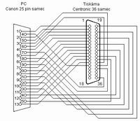
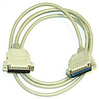
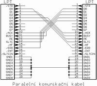
Linkage of mostly used cabels
Tiskový kabel
(Centronic)
Použití: připojení tiskárny k LPT portu. |
Redukce
Centronic - LapLink
Použití: spojení dvou PC tiskovým kabelem (Centronic) jako LapLinkovým |
LapLink
kabel
Použití: propojení dvou PC |
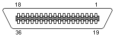
25 pin D-sub connector
(into PC )
36 pin Centornics connector
(into printer)
Name |
25-DSub |
36-Cen |
| Strobe |
1 |
1 |
| Data Bit 0 |
2 |
2 |
| Data Bit 1 |
3 |
3 |
| Data Bit 2 |
4 |
4 |
| Data Bit 3 |
5 |
5 |
| Data Bit 4 |
6 |
6 |
| Data Bit 5 |
7 |
7 |
| Data Bit 6 |
8 |
8 |
| Data Bit 7 |
9 |
9 |
| Acknowledge |
10 |
10 |
| Busy |
11 |
11 |
| Paper Out |
12 |
12 |
| Select |
13 |
13 |
| Autofeed |
14 |
14 |
| Error |
15 |
32 |
| Reset |
16 |
31 |
| Select |
17 |
36 |
| Signal Ground |
18 |
33 |
| Signal Ground |
19 |
19,20 |
| Signal Ground |
20 |
21,22 |
| Signal Ground |
21 |
23,24 |
| Signal Ground |
22 |
25,26 |
| Signal Ground |
23 |
27 |
| Signal Ground |
24 |
28,29 |
| Signal Ground |
25 |
30,16 |
| Shield |
Shield |
Shield+17 |
For higher resolution click on the figure |
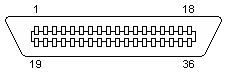
36 pin Centornics connector
(into printer cabel from PC 1)
25 pin D-sub connector
(into PC 2)
| Name |
Cen |
DSub |
Name |
| Data Bit 0 |
2 |
15 |
Error |
| Data Bit 1 |
3 |
13 |
Select |
| Data Bit 2 |
4 |
12 |
Paper Out |
| Data Bit 3 |
5 |
10 |
Acknowledge |
| Data Bit 4 |
6 |
11 |
Busy |
| Acknowledge |
10 |
5 |
Data Bit 3 |
| Busy |
11 |
6 |
Data Bit 4 |
| Paper Out |
12 |
4 |
Data Bit 2 |
| Select |
13 |
3 |
Data Bit 1 |
| Error |
32 |
2 |
Data Bit 0 |
| Reset |
16 |
16 |
Reset |
| Select |
17 |
17 |
Select |
| Signal Ground |
19-30+33 |
18-25 |
Signal Ground |
|
25 pin D-sub connector
(into PC 1)
25 pin D-sub connector
(into PC 2)
| Name |
Pin |
Pin |
Name |
| Data Bit 0 |
2 |
15 |
Error |
| Data Bit 1 |
3 |
13 |
Select |
| Data Bit 2 |
4 |
12 |
Paper Out |
| Data Bit 3 |
5 |
10 |
Acknowledge |
| Data Bit 4 |
6 |
11 |
Busy |
| Acknowledge |
10 |
5 |
Data Bit 3 |
| Busy |
11 |
6 |
Data Bit 4 |
| Paper Out |
12 |
4 |
Data Bit 2 |
| Select |
13 |
3 |
Data Bit 1 |
| Error |
15 |
2 |
Data Bit 0 |
| Reset |
16 |
16 |
Reset |
| Select |
17 |
17 |
Select |
| Signal Ground |
25 |
25 |
Signal Ground |
For higher resolution click on the figure
|
| Rules for making communication cables |
For an every data cabel and for parallel cabels two-times
important is shielding. Every data line should has its ground line
(GND) side by side or should be shielded. So it's possible to avoid
crosstalks between lines. It means possible higher data rate and communication
on further distance. If a flat cabel is used, the wiring will be done
by structure of the cabel and port. If wires budle is used, every
data line should be twisted with signal ground line. Shielding of
all twisted pairs makes the parameters better.
LPT communication modes
| SPP Mode - Compatibility Mode |
This mode is also called Centronics mode and it is standard
mode for parallel data communication. It was originally intended only
for communication PC with printer. There is defined only forward data
transfer, it means from a PC to a peripheral device and data rate
can be only to 150kbps. Communication process is described in following
figure 3.

Fig. 3. Compatibility Mode (SPP mode) Data Transfer
Cycle
Compatibility Mode phase transitions:
- Write the data to the data register
- Program reads the status register to check that the printer is
not BUSY
- If not BUSY, then Write to the Control Register to assert the
STROBE line
- Write to the Control register to de-assert the STROBE line
In nowadays, many of the integrated 1284 I/O controllers have implemented
Fast Centronics or Paralel Port FIFO Mode, which use FIFO buffers
for data transfer. Then data written in FIFO port are transfered to
printer using hardware generated handshake signals and it increases
data rate up to 500KBbs. However this mode isn't defined in standard
IEEE 1284.
SPP Register Interface
The basic SPP mode of parallel port is controled by 3 base
registers:
- Data Register - intended for writing of transmit data určený pro
zápis vysílaných dat
- Status Register - intended for reading states on the lines.
- Control Register - intended for controlling of the peripherial
device, which receives transmitted data.
Pins allocation to bits in registers is in the following figure 4.
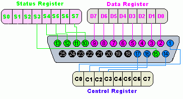
Fig. 4. Bits allocation in the LPT parallel port
| Offset |
Name |
Read/Write |
Bit No. |
Properties |
| Base + 0 |
Data Port |
Write |
Bit 7 |
Data 7 |
| Bit 6 |
Data 6 |
| Bit 5 |
Data 5 |
| Bit 4 |
Data 4 |
| Bit 3 |
Data 3 |
| Bit 2 |
Data 2 |
| Bit 1 |
Data 1 |
| Bit 0 |
Data 0 |
Tab 4. Data Register
On base address there is data register for transmitting of the
8-bit value on lines. The register is intended only for writing.
Reading is possible, but it is read only last transmited byte.
| Offset |
Name |
Read/Write |
Bit No. |
Properties |
| Base + 1 |
Status Port |
Read Only |
Bit 7 |
Busy |
| Bit 6 |
Ack |
| Bit 5 |
Paper Out |
| Bit 4 |
Select In |
| Bit 3 |
Error |
| Bit 2 |
IRQ (Not) |
| Bit 1 |
Reserved |
| Bit 0 |
Reserved |
Tab. 5. Status Register
Status register with address base +1 is intended for reading and
describes state of the communicating device (printer).
| Offset |
Name |
Read/Write |
Bit No. |
Properties |
| Base + 2 |
Control Port |
Read/Write |
Bit 7 |
Unused |
| Bit 6 |
Unused |
| Bit 5 |
Enable Bi-Directional Port |
| Bit 4 |
Enable IRQ Via Ack Line |
| Bit 3 |
Select Printer |
| Bit 2 |
Initialize Printer (Reset) |
| Bit 1 |
Auto Linefeed |
| Bit 0 |
Strobe |
Tab. 6. Control Register
Control register (Tab. 6) is designated for writing and it enables to control of communicating device (printer)
by the 5 output bits.
Nibble mode is way how to get reverse channel and bidirectional
communication between peripherial device and PC directly from classical
SPP Compatible mode without hardware adjustment. It is neccesary only
software support. Therefore the data rate limit is up to 100kbps.
The advantage is ability of bidirectional communication on all PCs
with LPT.
For transfer it is used 5 inputs lines of PC port which are intended
for the handshake. The four ones are used for data transfer into PC.
Using of these lines the periphery can transmit byte as sequence of
2 nibbles (4 bits) in two followings data cycles. Both cycles decribe
figure 5. and table 7.
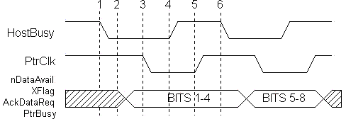
Fig. 5. Byte Mode Data Transfer Cycle
| SPP Signal |
Nibble Mode
Name |
In/Out |
Description -- Signal usage
when in Nibble Mode data transfer |
| nSTROBE |
nSTROBE |
Out |
Not used for reverse data transfer |
| nAUTOFEED |
HostBusy |
Out |
Host nibble mode handshake signal. Set low to indicate host is ready
for nibble. Set high to indicate nibble has been received. |
| nSELECTIN |
1284Active |
Out |
Set high when host is in a 1284 transfer mode. |
| nINIT |
nINIT |
Out |
Not used for reverse data transfer |
| nACK |
PtrClk |
In |
Set low to indicate valid nibble data, set high in response to HostBusy
going high. |
| BUSY |
PtrBusy |
In |
Used for Data bit 3, then 7 |
| PE |
AckDataReq |
In |
Used for Data bit 2, then 6 |
| SELECT |
Xflag |
In |
Used for Data bit 1, then 5 |
| nERROR |
nDataAvail |
In |
Used for Data bit 0, then 4 |
| DATA[8:1] |
Not Used |
|
|
Tab. 7. Nibble Mode Signals
After implementation of parallel port interface, some producers
in the lead with IBM increase transfer capacity by removing data lines
drivers and provide bidirectional 8-bit communication by way of data
lines. Then data rate is up to 200kbps. Figure 6. shows one transfer
cycle in this mode and table 8. describe particular signals.
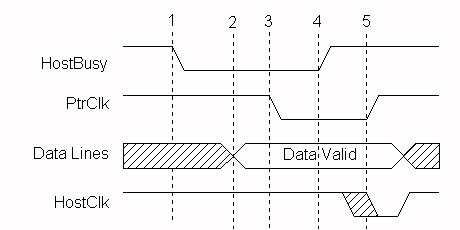
Fig. 6. Časový průběh komunikace v obousněrném Byte módu
| SPP Signal |
Byte Mode Name |
In/Out |
Description
Signal usage when in Byte Mode data transfer |
| nSTROBE |
HostClk |
Out |
Pulsed low at the end of each Byte mode data transfer to indicate that
the byte was received. Acknowledge signal. |
| nAUTOFEED |
HostBusy |
Out |
Set low to indicate host is ready for byte. Set high to indicate byte
has been received. Handshake signal. |
| nSELECTIN |
1284Active |
Out |
Set high when host is in a 1284 transfer mode. |
| nINIT |
nINIT |
Out |
Not used. Set high. |
| nACK |
PtrClk |
In |
Set low to indicate valid data on the data lines, set high in response
to HostBusy going high. |
| BUSY |
PtrBusy |
In |
Forward channel Busy status. |
| PE |
AckDataReq |
In |
Follows nDataAvail |
| SELECT |
Xflag |
In |
Extensibility flag. Not used in Byte mode. |
| nERROR |
nDataAvail |
In |
Set low by peripheral to indicate that reverse data is available. |
| DATA[8:] |
DATA[8:1] |
Bi-Di |
Used to provide data from peripheral to host. |
Tab. 8. Byte Mode Signals
EPP - Enhanced Parallel Port protocol was originally developed
by companies Intel, Xircom and Zenith Data Systems to provide powefull
connection through parallel port and still was compatible with standard
LPT. This protocol was for the first time implemented in 386SL chipset
(82360 I/O chip). After this it became a part of the IEEE 1284 standard.
The effect of this mode is data rate between 500kbps and 2Mbps. The
transfer is as fast as data rate of the slowest communicating devices.
The rate is found from changings of messages and responses from handshake
signals nWait and nDataStrobe ( figure 7.).
EPP protocol provides 4 transfer cycles:
- Data Write Cycle
- Data Read Cycle
- Adress Write Cycle
- Adress Read Cycle
Data cycles are intended for data transfer between PC and peripherials.
Address cycles are intended for channel address tranfer or command
and control information. Both are neccessery to show as two different
transfer cycles.
| SPP Signal |
EPP Signal Name |
In/Out |
EPP Signal Description |
| nSTROBE |
nWRITE |
Out |
Active low. Indicates a write operation High for a read cycle. |
| nAUTOFEED |
nDATASTB |
Out |
Active low. Indicates a Data_Read or Data_Write operation is in process. |
| nSELECTIN |
nADDRSTB |
Out |
Active low. Indicates an Address_Read or Address_Write operation is in process. |
| nINIT |
nRESET |
Out |
Active low. Peripheral reset. |
| nACK |
nINTR |
In |
Peripheral interrupt. Used to generate an interrupt to the host. |
| BUSY |
nWAIT |
In |
Handshake signal. When low it indicates that is OK to start a cycle (assert
a strobe), when high it indicates that it is OK to end the cycle (de-assert
a strobe). |
| D[8:1] |
AD[8:1] |
Bi-Di |
Bi-directional address/data lines. |
| PE |
user defined |
In |
Can be used differently by each peripheral |
| SELECT |
user defined |
In |
Can be used differently by each peripheral. |
| nERROR |
user defined |
In |
Can be used differently by each peripheral. |
Tab. 9. EPP mode signals Definitions
Figure 5. shows one of the data write cycle. CPU signal
nIOW emphasizes all handshake which come on one I/O cycles.
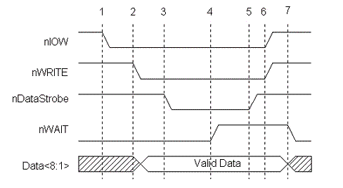
Fig. 7. EPP Data Write Cycle
Data Write cycle phase transitions:
- Program executes an I/O write cycle to port 4 (EPP Data Port)
- The nWrite line is asserted and the data is output to the parallel
port
- The data strobe is asserted, since nWAIT is asserted low
- The port waits for the acknowledge from the peripheral (nWAIT
deasserted - high)
- nDataStrobe is deasserted and the EPP cycle ends
- The ISA I/O cycle ends
- nWAIT is asserted low to indicate that the next cycle may begin
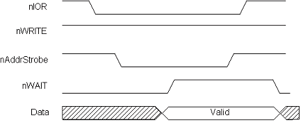
Fig. 8. EPP Address Read Cycle
Note : The parallel ports with EPP before standardization IEEE 1284
can have little bit different process of some handshake signals.
EPP Register Interface
The following table 10. describes extended registers in comparison
with SPP mode. As was written higher, SPP mode uses 3 basic registers:
Data, Status and Control Register. EPP mode extents them about several
new registers as it is in the table 10, which presents register offsets
from base port address.
| Port Name |
Offset |
Mode |
Read/Write |
Description |
| SPP Data Port |
+0 |
SPP/EPP |
W |
Standard SPP data port. No autostrobing. |
| SPP Status Port |
+1 |
SPP/EPP |
R |
Reads the input status lines on the interface. |
| SPP Control Port |
+2 |
SPP/EPP |
W |
Sets the state of the output control lines. |
| EPP Address Port |
+3 |
EPP |
R/W |
Generates an interlocked address read or write cycle. |
| EPP Data Port |
+4 |
EPP |
R/W |
Generates an interlocked data read or write cycle. |
| Not Defined |
+5 to +7 |
EPP |
N/A |
Used differently by various implementations. May be used for 16 and
32 bit I/O. |
Tab. 10. EPP Register Definitions
An easy attempt for writing on base address + 4 can find, if the
device supports this communation mode.
The Extended Capability Port, or ECP, protocol was proposed
by Hewlett Packard and Microsoft as an advanced mode for communication
with printer and scanner type peripherals. Data rate in this mode
can be up to 800KBps without using DMA ( Direct Memory Access) and
up to 2MBps with help of DMA. It's true in implementation on ISA bus.
Nowadays LPT interface implemented on PCI bus can reach up to 3 or
5 MBps. Sometimes it's presented possibility up to 8MBps.
The ECP protocol provides the following cycle types in both
the forward and reverse directions:
- Data cycles
- Command cycles
Full register implementation and description can be found in Microsoft
document: "The IEEE 1284 Extended Capabilities Port Protocol
and ISA Interface Standard" (ecp_reg.pdf).
This document defines features and implementation which IEEE 1284
standard doesn't appreciate. As example Run_Length_Encoding (RLE)
data compression, FIFO buffers, DMA and programming too.
RLE enables real-time data compression with ratio up to 64:1, but
it have to be permited on both communicating devices.
Plná registrová implementace a popis lze nalézt v dokumentu Microsoft:
"The IEEE 1284 Extended Capabilities Port Protocol and ISA Interface
Standard" (ecp_reg.pdf). Tento dokument
definuje vlastnosti a implementaci, které IEEE 1284 standard nepostihuje.
Jako například Run_Length_Encoding (RLE) datovou kompresi, FIFO buffery,
DMA i programování. It's advantageous for example in transfer
of large data amount of a picture from a scaner. Channel addressing
is different from EPP mode. The ECP addressing (Channel addressing)
is intended for addressing of many logical devices by one physical
device. For example to one parallel port are connected FAX, printer
and modem. Using ECP channel addressing it's possible accesses to
each one. So it's possible to receive data from the modem during the
time when data channel is busy because of printer printing.
In basic communication mode during busy signal from printer isn't
able to communicate with others devices. In ECP mode is enough only
to address other logical channel and communication can proceed. In
the same way as other extended modes ECP protocol redefines classical
SPP signals and adds other signals for ECP handshake.
| SPP Signal |
ECP Mode Name |
In/Out |
Description -- Signal usage when in ECP Mode data
transfer |
| nSTROBE |
HostClk |
Out |
Used with PeriphAck to transfer data or address information in the forward
direction. |
| nAUTOFEED |
HostAck |
Out |
Provides Command/Data status in the forward direction. Used with PeriphClk
to transfer data in the reverse direction. |
| nSELECTIN |
1284Active |
Out |
Set high when host is in a 1284 transfer mode. |
| nINIT |
nReverseRequest |
Out |
Driven low to put the channel in reverse direction. |
| nACK |
PeriphClk |
In |
Used with HostAck to transfer data in the reverse direction. |
| BUSY |
PeriphAck |
In |
Used with HostClk to transfer data or address information in the forward
direction. Provides Command/Data status in the reverse direction. |
| PE |
nAckReverse |
In |
Driven low to acknowledge nReverseRequest. |
| SELECT |
Xflag |
In |
Extensibility flag. |
| nERROR |
nPeriphRequest |
In |
Set low by peripheral to indicate that reverse data is available. |
| Data[8:1] |
Data[8:1] |
Bi-Di |
Used to provide data between the peripheral and host. |
Tab. 11. ECP Mode Signals
Figure 9 shows two forward data transfer cycles. When HostAck is
high it indicates that a data cycle is taking place. When HostAck
is asserted low, a command cycle is taking place and the data represents
either an RLE count or a Channel address. Bit 8, of the data byte
is used to indicate RLE vs. Channel address. If bit 8 is 0, then bits
1-7 represent a Run_Length Count (0-127). If bit 8 is 1, then bits
1-7 represent a Channel address (0-127).
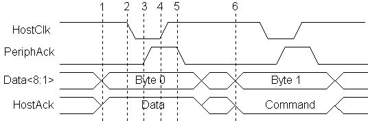
Fig. 9. ECP Forward Data and Command Cycle
Note: Because in ECP mode FIFO buffers are used, it's necessary
to point out that receiving device has valid data in FIFO buffer in
time point 4, thus after pass of signal HostClk in high level. Between
points 3 and 4 it's possible to interrupt trasfer. Then it isn't guaranteed
that data was successfully transfered.
Figure 10 shows a reverse channel command cycle followed
by a reverse channel data cycle. The I/O read or write strobes are
not shown in these figures. This is because the ECP FIFOs are used
to decouple the ISA data transfers, either DMA or programmed I/O,
from the actual host/peripheral data transfers. It is this decoupling
of the transfer states that makes the ECP protocol a "loosely
coupled" protocol. The software driver does not know the exact
state of the data transfers. If a large block is being transferred
via DMA, the driver does not know if the 123rd byte is being transferred
or the 342,201st byte. As in the case of printers, the software may
not care. The only concern is whether the transfer was completed or
not. Therewithal this picture shows differents between ECP mode ans
EPP mode. In EPP mode software can mixes mode of reading and writing
on line. On the contrary in ECP mode device have to inquire of reverse
data transfer with help of signals nReverseRequest a nAckReverse.
Then have to wait for finishing DMA transfer or interrupt from DMA.
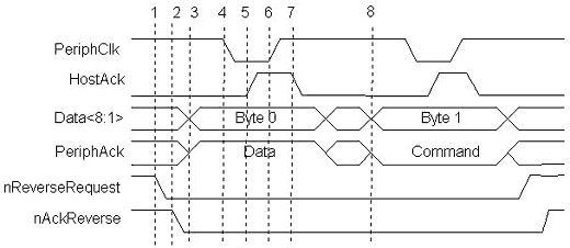
Fig. 10. ECP Reverse Data and Command Cycle
ECP Software and Register Interface
The Microsoft specification, "The IEEE 1284 Extended
Capabilities Port Protocol and ISA Interface Standard", defines
a common register interface for ISA based 1284 adapters with ECP.
This specification also defines a number of operational modes that
the adapter can operate under. Table 12 identifies these modes.
| Mode |
Description |
000 |
SPP mode |
001 |
Bi-directional mode (Byte mode) |
010 |
Fast Centronics |
011 |
ECP Parallel Port mode |
100 |
EPP Parallel Port mode |
101 |
(reserved) |
110 |
Test mode |
111 |
Configuration mode |
Tab. 12. ECR Register Modes (they set in ECR register - previous
Tab. 13.)
Note: The EPP mode isn't specified by ECP
protocol, but it's implemented in most controllers.
The ECP Register model comes out from standard parallel
port, but it defunes 6 registers which describes the following table
13. Important register definition depends on just settings of the
ECP mode ( previous table 12.).
| Offset |
Name |
Read/Write |
ECP
Mode |
Function |
| 000 |
Data |
R/W |
000-001 |
Data Register |
| 000 |
ecpAfifo |
R/W |
011 |
ECP Address FIFO |
| 001 |
dsr |
R/W |
all |
Status Register |
| 002 |
dcr |
R/W |
all |
Control Register |
| 400 |
cFifo |
R/W |
010 |
Parallel Port Data FIFO |
| 400 |
ecpDfifo |
R/W |
011 |
ECP Data FIFO |
| 400 |
tfifo |
R/W |
110 |
Test FIFO |
| 400 |
cnfgA |
R |
111 |
Configuration Register A |
| 401 |
cnfgB |
R/W |
111 |
Configuration Register B |
| 402 |
ecr |
R/W |
all |
Extended Control Register |
Tab. 13. ECP
Register Description
From reason of the topic comprehension, I won't describe
particular bit definition in each from 6 registers. An interested
person can find it in a very detailed description of Microsoft specification:
"The Extended Capabilities Port Protocol and ISA Interface Standard",
which is a part of document ecp_reg.pdf,
or a datasheet of a particular I/O controller.
LPT Program Access
| DOS / Windows 95, 98, Me |
Windows NT4, 2000, XP |
For program access
under operating system MS-DOS, it's possible to use only direct
commands of programming language for direct access to LPT registers.
Commands
summary for direct access in Pascal, C, assembler x86 and Basic
language are released in the following text file
For program access under OS Windows 95/98/Me it's possible
to find a lot of universal drivers for common users and programmers
for direct access under Windows 95/98. For example:
- port.dll - port.zip - very good driver for access in Windows 95/98/Me. Driver
is also part of CD-ROM in the czech book: Burkhard Kainka,
Hans-Joachim Berndt : Využití rozhraní PC pod Windows,
it's shopped by BEN. The book contains a lot of practical
source programs for Visual Basic and Delphi.
|
With coming of OS
Windows based on NT core, it appears problems with parallel
port access. Programs written with classical direct access to
LPT, which works under OS DOS and Windows95/98, will not work
properly. This programs can't be used, because they show an
error message like "The exception privileged instruction
occurred in the application at location ...." and they
are interrupted. It's caused by Windows NT/2000/XP security
for being more stable system. Windows NT assigns some privileges
and restrictions to different types of programs running on it.
It classifies all the programs in to two categories , User mode
and Kernel mode, running in ring3 and ring0 modes. Generally
written programs running in User mode aren't allowed to access
to LPT port using certain instructions like IN, OUT etc.. Whenever
the operating system find that a user mode program is trying
to execute such instructions, the operating system stops execution
of those programs and will display an error message .In Kernel
mode isn't such restrictions so it is neccessary to use a driver
which runs there. Then the driver can be used for LPT port access
by the program which access needs.
Because writing a such driver isn't an easy job, at the internet
is possible to find a lot of univesal drivers for users and
programmers requirements. They usually allows to write and read
data from LPT sometimes some other features. For example:
I tested each driver for writing and reading to LPT port with
address 0x378 in programming language C++ (program C++ Builder
5).
Here
is source program which can be used as an example of using dll
drivers in C++ programs. |
| For older programs under
Windows NT4/2000/XP |
| Generally |
Some programs |
As it was mentioned
higher, every program uses access to PC parallel port, which
was programmed for OS DOS and Windows 95/98, can't work alone
and independent on OS Windows. Under Windows NT/2000/XP should
be used some universal program which runs on background of Windows
and enables running older programs with direct access to LPT
port. |
- UserPort - userport.zip
- program for access to LPT port under Windows 2000/XP
for older otherwise functionless programs (pack also contains
source program with drivers for Windows) .
- PortTalk - porttalk22.zip - program for access to LPT port under Windows 2000/XP for
older otherwise functionless programs. Pack also contains
source program with drivers for Windows including an example
of access in C language.
Note: Both programs was tested as functional under
Windows XP |
LPT Control Programs
| DOS / Windows 95, 98, Me |
Windows NT4, 2000, XP |
- Ka - ka.zip - program
for reading and setting pins of parallel port + next operations
(generator TTL etc.), program works under Windows XP, too.
|
- DLPortIO - port95nt.exe
- program for data (Byte or Word) reading and writing
to selected LPT port (pack contains drivers for Windows).
|
Note : Here presented programs was tested as fully functional
under OS Windows 98 or XP (Programy zde uvedené byly odzkoušeny jako
plně funkční v OS Windows 98 nebo XP (according to program).
| Generally |
LPT (IEEE
1284) port and communication offer very easy using, because
communication uses classical TTL signals. That enables
making low cost interface for every device communicates
with PC. It's only neccessary to use a I/O buffer for
PC LPT port protection, some 8-bit buffer / driver (for
example 74LS244, 74LS367 / UL2803 or 8-bit shifter ( 74HC165).
If you want to use all advantages and IEEE 1284 protocol
modes, it necessery to take a special integrated circuit
like circuits in the next list. |
|
| IEEE 1284 Integrated Circuits datasheets |
|
|
DOWNLOAD & Links
|
| Documentation |
- Detailed LPT pins description (1page) - pppinout.pdf
- Detailed parallel port description and its
modes (17 pages) - parallel.pdf
- Very detailed LPT ECP mode description with
registers description. (53 pages) - ecp_reg.pdf
|
|
|
LPT Literature in Czech
- Götz Sören, Mende Reiner : Měření, řízení a regulace s Delphi,
BEN 2004 - LPT port and EPP mode description with examples
- Matoušek David : Udělejte si z PC... 1. díl , BEN 2004
- program access to LPT port under Windows and DOS
- Matoušek David : Udělejte si z PC v Delphi..., 1.díl, BEN
2003 - program access to LPT port in SPP mode
- Matoušek David : Udělejte si z PC... 2. díl , BEN 2004
- LPT port in standard SPP/EPP/ECP
- Burkhard Kainka, Hans-Joachim Berndt : Využití rozhraní PC
pod Windows, HEL 2000 - using LPT port under Windows 95/98
- Vlach Jaroslav : Počítačová rozhraní, BEN 2000 - LPT port
general description
Next Interesting Links
Pages on HW Serveru
Web pages in english:
Web pages in czech:
Web pages in german:
|