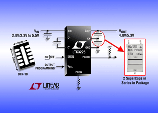
The device employs a low-noise charge-pump architecture to charge two supercapacitors in series to a fixed output voltage (4.8V/5.3V selectable) from a 2.8V to 5.5V input supply. Charge current is resistor programmable up to 150mA, and the device’s automatic cell balancing feature maintains equal voltages on both cells (2.4V/2.65V selectable) without requiring balancing resistors.
This protects each supercapacitor from overvoltage damage caused by mismatches in cell capacitance or leakage while minimizing current drain on the capacitors. The LTC3225 will not discharge the supercapacitors when the input supply is removed or shorted to ground.
The LTC3225 operates with a very low 20uA quiescent current when the output voltage is in regulation and draws only 2uA from VOUT. Current is further reduced when the input supply is removed as the IC automatically enters a low current shutdown state, drawing less than 1uA from the supercapacitors. The basic charging circuit requires only 3 external components and takes up little space; the IC is offered in a tiny 6mm2 footprint DFN package. It is ideal for current-limited applications with high peak power loads such as LED flash PCMCIA Tx bursts, HDD bursts, and GPRS/GSM transmissions; in addition it may be used as a backup supply. Also, bigger board-level systems such as servers and RAID/mass storage systems often have a need for brief high-power backup supplies for which supercapacitors are well-suited.

| Summary of Features: LTC3225 | |
| Low Noise, Constant Frequency Charging of Two Series Supercapacitors | |
| Automatic Cell Balancing Prevents Capacitor Overvoltage During Charging | |
| Programmable Charging Current (Up to 150mA) | |
| Selectable 2.4V or 2.65V Regulation per Cell | |
| Automatic Recharge | |
| IVIN = 20μA in Standby Mode | |
| No Inductors | |
| Current Limiting and Thermal Limiting | |
| Tiny Application Circuit, All Components < 1mm High | |
| Compact, Low-Profile (0.75mm) 2mm × 3mm 10-Lead DFN Package | |


